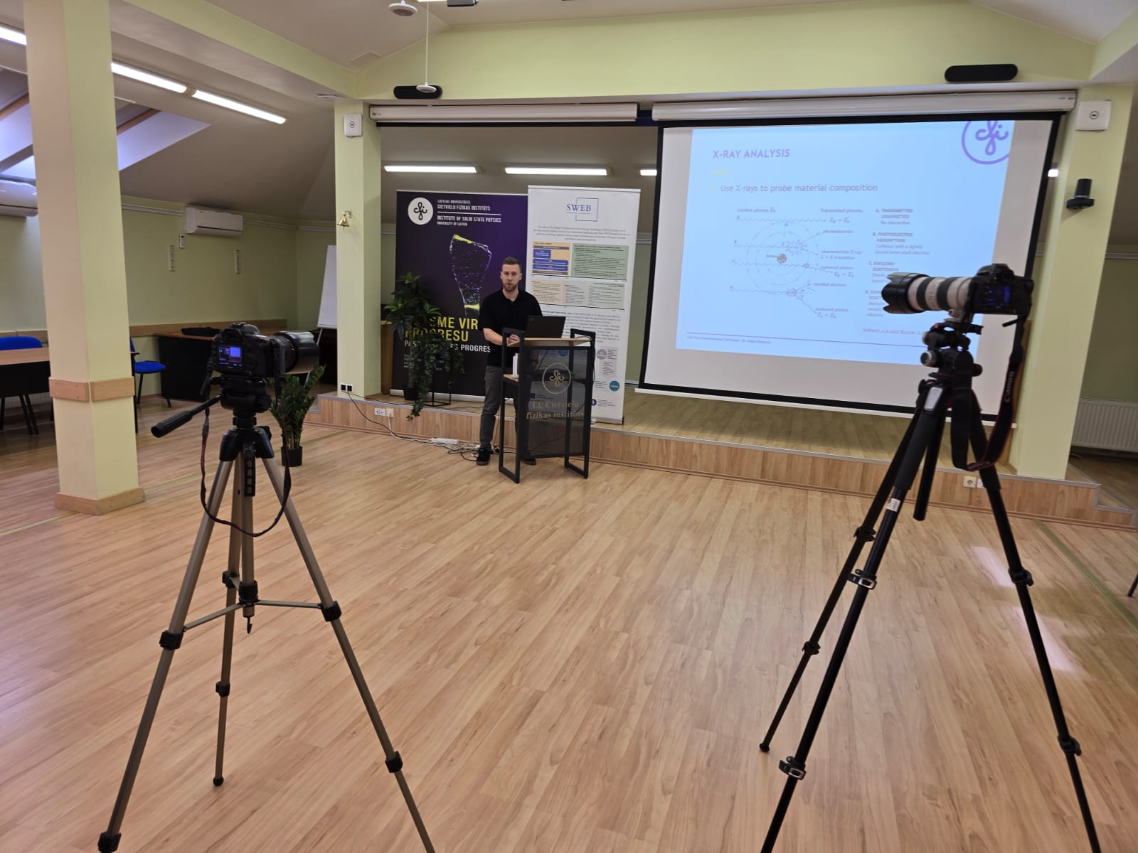
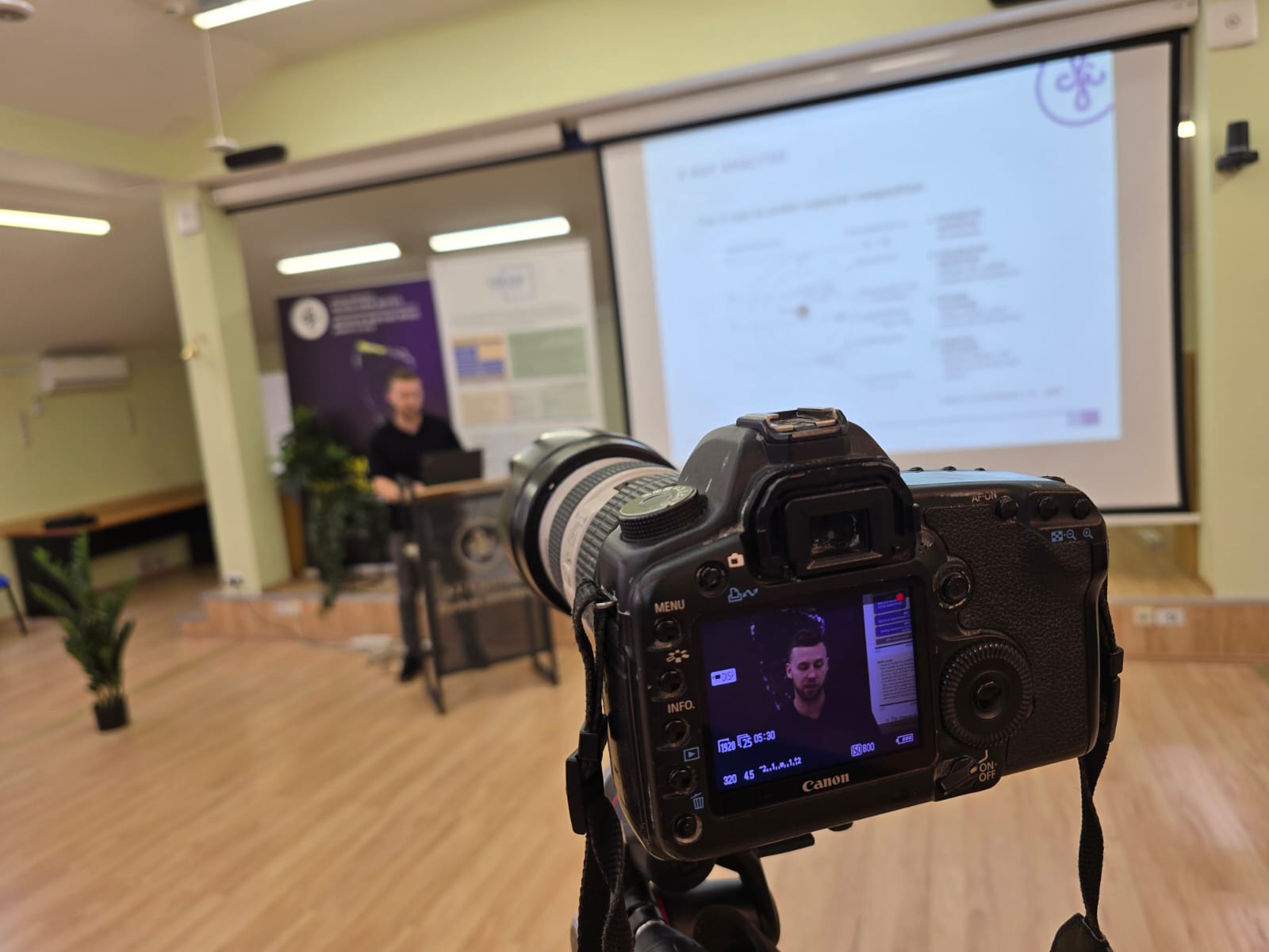
The cameras were rolling today at Latvijas Universitātes Cietvielu fizikas institūts / the Institute of Solid State Physics, University of Latvia (ISSP UL), as Dr. Edgars Butanovs, Head of the Semiconductor Thin Film Nanotechnology Group, guided us into the fascinating world of Thin Film Characterization Techniques.
From semiconductors and optical materials to advanced analytical methods, Dr. Edgars Butanovs unpacked the tools and insights that help scientists see beyond the coatings’ surface, literally paving the way for breakthroughs in smart windows, renewable energy, and sustainable construction.
This episode is more than just a lecture. It’s part of the Smart Windows for Zero Energy Buildings (SWEB) project’s mission under the European Research Area to open our research to the world, sharing knowledge freely, encouraging collaboration without borders, and equipping the next generation of innovators. By making advanced scientific methods accessible through our Open Science video series, we’re building skills, sparking curiosity, and accelerating Europe’s path to climate neutrality.